

設計から完成まであらゆるニーズにお応えする基板のデザインを提供
- ●半導体テスト用の前工程・後工程用基板の設計・製造・販売
- ●テスト用汎用基板
- ●バーインボード及び周辺機器の設計・製造・販売
- ●研究機関、大学で使用する特殊な基板
- ●各種カスタム基板
- ●We provide all custom board from board design to completed boards
- ●Performance board(Load board)
- ●Probe card
- ●Standard board
- ●Burn-in board and peripheral equipment
- ●Special characteristics boards for R&D/University
標準作業手順Standard work flow procedure.
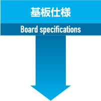
- ■弊社にて仕様検討
基板の層構成、注意点など
御見積書の提示 Consider the board specifications.
Board layer structure and notes.
Provide the quotation and lead-time.
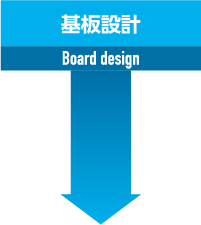
- ■回路設計及び部品配置図
基板設計(配線) Schematic diagram, layout and device location.
Board design by using CAD.

- ■お客様で図面の最終確認、弊社からのご説明も可能です We describe the our board design.

- ■CADデータの最終確認Confirm the CAD data by using CAM
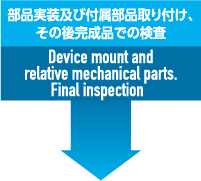
- 部品調達から実装まで可能です
機構部品も製作します。
実装はリフロー及び手はんだです。 - We purchase the devices and device mount by reflow and hand soldering.

- ■御指定場所に国内だけではなく海外にもお送りします。 Deliver worldwide locations.
主なお取引先様
■国内外の半導体メーカー、半導体製造会社、半導体テスト会社、電気・電子機器メーカー、研究所、国立研究開発機関、大学 など
Major customers are Semiconductor manufacturers, Test house, Electronics manufacturers, R&D, National research & development agency, University and others.
主な設計環境Design tools
・Allegro, OrCAD, CadvanceαIII ・SPECCTRAQuest シミュレーションソフト ・UCAM ほか
Web会議システムWeb conference system
Web会議で遠くに離れた場所でも素早く会議を行い、短納期での対応が可能です。
 国内外の主要テスタに対応